// NATURE NEWS — SPAZIO & SCIENZA
Electroluminescent photoresists extending lithographic scaling to OLEDs
Nature
(2026) Cite this article
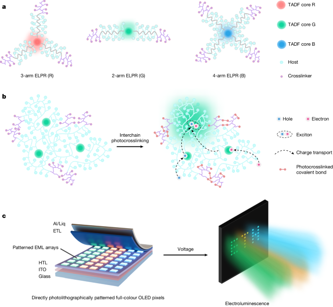
The miniaturization of organic light-emitting diodes is critical for next-generation ultrahigh-resolution displays and integrated photonics1,2,3,4,5,6,7,8. However, traditional vacuum evaporation and inkjet printing methods are incompatible with the lithographic scaling processes that underpin silicon electronics9,10,11,12,13,14,15,16, hindering true monolithic integration with complementary metal–oxide–semiconductor circuits. Here we present electroluminescent photoresists synthesized via atom transfer radical polymerization that can be directly patterned by ultraviolet and electron-beam lithography. These multi-arm star polymers feature a core–shell architecture designed to embed the thermally activated delayed fluorescence emitters within a protective host shell, segregating them from the reactive photocrosslinking moieties on the surface. The site-specific isolation ensures that crosslinking reactions occur at the periphery, leaving the emissive cores intact and preserving high electroluminescence. We demonstrate robust processing orthogonality in sequential multilayer electroluminescent photoresist photolithography, enabling subdiffraction fluorescence nanopatterns with critical dimensions down to 110 nm. We validate their device performance with multicolour, ultraviolet-patterned organic light-emitting diodes exhibiting external quantum efficiencies exceeding 13%. These results not only pave the way for extending Moore’s law to organic optoelectronics but also unlock their potential for monolithic optoelectronic integration.
The monolithic integration of high-performance light sources with silicon-based complementary metal–oxide–semiconductor (CMOS) electronics is a cornerstone for next-generation optoelectronics1, promising to revolutionize augmented-reality microdisplays2, optical computing3 and high-speed on-chip interconnects4,5. Although inorganic III–V semiconductor devices have dominated research in this field, their integration remains fundamentally constrained by lattice mismatch, the requirement for high-temperature epitaxy6,7 and the yield-limiting complexity of heterogeneous transfer processes8. Furthermore, as pixel size scales into the sub-10-μm regime, inorganic emitters suffer from severe efficiency roll-off owing to non-radiative recombination at sidewall defects17,18,19,20. In this regard, organic semiconductors emerge as a compelling alternative21,22. For example, in organic light-emitting diodes (OLEDs), their amorphous emissive layers, coupled with low-temperature and lattice-free fabrication, enable direct back-end-of-line compatible processing on CMOS wafers while preserving high external quantum efficiencies (EQEs) independent of device dimensions23.
Despite these material virtues, a viable technical roadmap towards the monolithic integration of multicolour OLEDs remains elusive24. The primary bottleneck lies in the chemical fragility of organic semiconductors, which are readily degraded by the solvents and developers inherent to standard photolithography21,25. Consequently, current manufacturing methods, such as fine-metal-mask evaporation and inkjet printing, are fundamentally limited by their restricted spatial resolution and overlay accuracy9,10,26. More critically, these techniques are inherently decoupled from subsequent photolithographic processes, preventing OLED technology from aligning with the rigorous integration densities and scaling laws dictated by modern silicon circuitry.
The development of directly photolithographically patternable organic emissive layers (EMLs)—a material system we formalize here as electroluminescent photoresists (ELPRs)—was first envisioned in the early 2000s to enable the multicolour integration of solution-processed polymer OLEDs11,12. Initial attempts utilized π-conjugated polymers with oxetane side groups synthesized via random polycondensation, forming insoluble networks through acid-catalys